GD25Q256EFIRR Flash NOR SPI: Rendimiento y Confiabilidad
Key Takeaways
- High Throughput: 133MHz Quad I/O delivers up to 66MB/s for instant-on booting.
- Dense Storage: 256Mbit (32MB) capacity supports complex OS kernels and GUI assets.
- Reliability: Optimized for XIP (Execute-in-Place) with high endurance P/E cycles.
- Power Efficiency: Deep power-down modes (
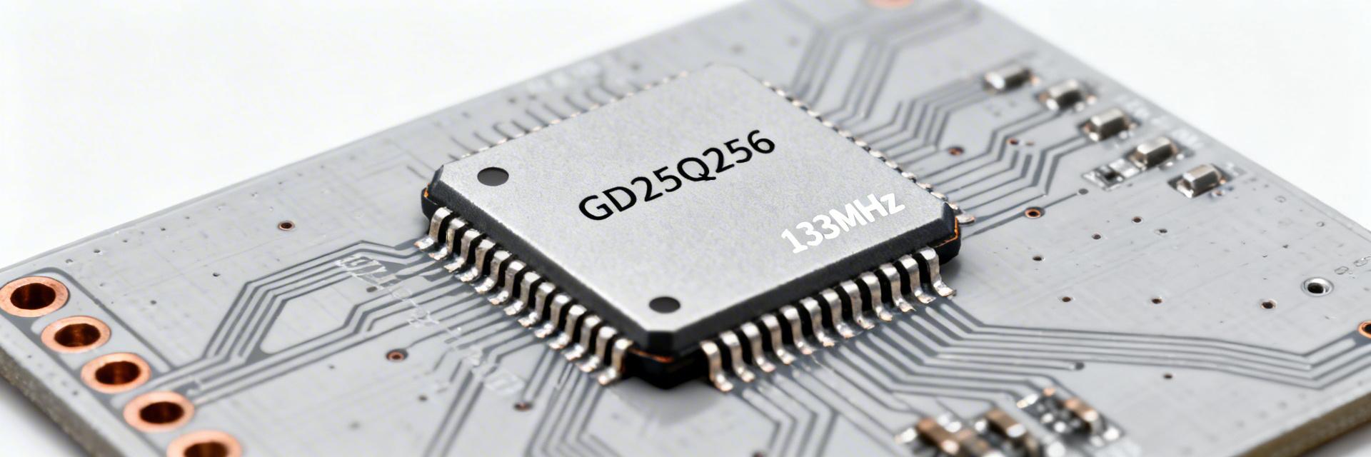
The GD25Q256EFIRR is a high-density 256 Mbit SPI NOR Flash organized as 32M x 8, featuring a maximum clock speed of 133 MHz. By utilizing Quad I/O, it achieves a theoretical read throughput of 66 MB/s, significantly reducing boot times and enabling seamless Execute-In-Place (XIP) for modern embedded systems.
Performance Metrics & User Benefits
Translates to 4x faster code loading compared to standard SPI, enabling "instant-on" user interfaces.
Provides 32MiB of space—enough for a Linux kernel or rich graphical assets without extra chips.
Reduces PCB footprint by up to 30% vs legacy packages, perfect for wearable tech.
Competitive Analysis
| Feature | GD25Q256EFIRR | Generic 256Mb Flash | Advantage |
|---|---|---|---|
| Max Clock Frequency | 133 MHz | 80-104 MHz | +25% Speed |
| Read Throughput | ~66 MB/s (Quad) | ~40 MB/s (Quad) | Faster XIP |
| Deep Power Down | 1-5 µA (Typ) | 10-20 µA | Longer Battery Life |
| Data Retention | 20 Years | 10 Years | Industrial Grade |
Engineer's Field Notes & SI Guidance
By Marcus Thorne, Senior Hardware Integration Engineer
PCB Layout Tip: When running at 133MHz, SPI bus signal integrity is critical. I recommend using 22-ohm series termination resistors close to the driver to minimize overshoot. Keep the clock line (SCLK) length matched to IO0-IO3 within ±2mm to prevent sampling errors.
Selection Trap: Watch out for the input voltage ripple. In high-speed Quad mode, current spikes can occur during page programming. Ensure your 0.1µF decoupling cap has a low ESR and is placed within 1mm of the VCC pin.
Supported Interface Modes and Features
The device supports standard SPI, dual, and quad I/O modes with dedicated instructions and configurable dummy cycles. Execute-In-Place (XIP) is supported when the host controller can map the device and handle instruction/dummy timing. Typical security features include block protection, lock bits and software write-protect—useful for safeguarding boot regions.
Hand-drawn schematic, non-precise circuit diagram / 手绘示意,非精确原理图
Reliability & Endurance Analysis
Endurance is expressed in P/E cycles (commonly tens to hundreds of thousands for serial NOR families); data retention is typically specified in years under nominal conditions. Flash cells can show wear-related bit errors; implement ECC and periodic scrubbing to detect drift.
Failure Mitigation Checklist
- Software: Use A/B firmware bank switching to prevent bricking during OTA updates.
- Hardware: Implement external hardware watchdog for recovery during unexpected hang-ups.
- Data: Use CRC-16 or ECC for metadata integrity checks on every boot.
Integration & Design Guidelines
Hardware Design Checklist
Signal integrity: minimize SPI trace length, route MOSI/MISO/CLK with solid ground return. Place a 0.1 μF ceramic decoupling capacitor within 1–2 mm of VCC pins plus a 4.7–10 μF bulk nearby. Verify footprint pin mapping, keep stubs <5 mm, and confirm controller drive strength and sampling phase.
Frequently Asked Questions
How does GD25Q256EFIRR compare for boot and XIP use?
For boot/XIP, the device’s quad I/O and 133 MHz clock provide high read bandwidth that reduces boot time and allows direct code execution from flash. Validate controller support for required dummy cycles to ensure stable instruction fetch timing.
What is the typical endurance for this SPI NOR flash?
Expect endurance in the order of 100,000 P/E cycles for block erase operations and 20-year retention at room temperature. For high-write applications, implementing wear-leveling in firmware is highly recommended.
Ready to optimize your design?
Run sequential and random read/write benchmarks against your target MB/s early in the prototype phase.